Pierre-Yvan Liardet
|
0
|
January 9, 2023


Side-channel and IoT or mobile devices: a real threat? To what extent a complex SoC, with multiple cores, cache memories, pipelining, …, can be a realistic target for a hardware attack? Are the operating frequency in gigahertz, or the technology, today in nanometers, real obstacles for side-channel experts? In this blogpost I will share our experiments on this topic with one objective: recover the secret key involved in the encryption or decryption of a single image taken with the camera of my phone. According to literature, this two megabyte image does not represent enough data to lead to the secret key recovery with a side-channel attack…
Among all solutions deployed in IoT and Mobile, one is ubiquitous: the ARM Cortex A-50 and A-70 core series. These cores leverage the ARMv8 instruction with possibly dedicated hardware instructions to implement AES encryption/decryption. This will be our target. In the following we present the target of our study in the context of a complex SoC, deliver what we learned from ElectroMagnetic (EM) signal observation and analyze the impact of the micro-architecture. Then, we show the result of a straightforward attack and also illustrate results obtained with a pipelined implementation.
Do you think we will decrypt this few megabytes image?

Figure - Encrypted image.
To find the place where and when an AES encryption or decryption is involved in an application is not straightforward. Indeed, on the following diagram we can realize that a typical Android software stack to go through in a file encryption, or decryption command, is far to be simple and unique.
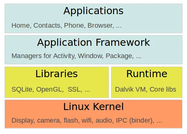
Figure - Android software stack.
Obviously, it seems hard to control the resources used by an application, especially because we can imagine that cryptographic services are populated by several libraries in many forms. On the same SoC we may have pure software, or dedicated hardware implementations, used according to the context coming from the applicative one, or the hardware available one. At some point, a decision to use this or this implementation is taken. My first attempt to address this topic shows that we have enough material for another blogpost, but from a more developer oriented perspective.
Nowadays, most of the phones are using ARM technology and there is a high probability that the application uses the ARMv8 dedicated AES instructions to encrypt the image.
So, to make things simple, and to leverage work already done by the team, we have decided to work with the Hisilicon Kirin 620 SoC (available on the Lemaker Hikey board) to target the ARMv8 instructions dedicated to AES. Indeed, we had this board on the shelf and have already developed sofware on it.
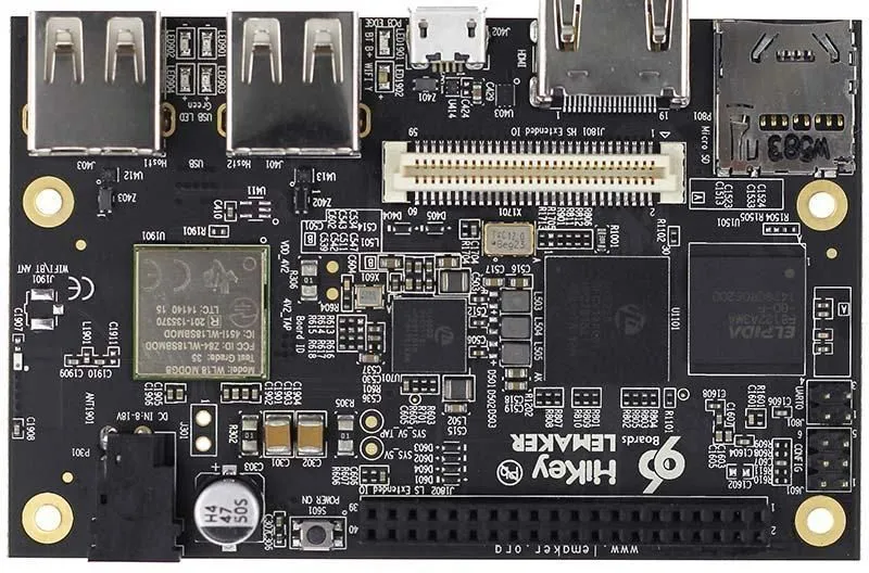
Figure - Hisilicon Kirin 620 SoC on the Hikey board.
To tell you a little bit about this, the ARMv8 instruction set is extended with Cryptographic Extensions (CE) including the two dedicated to AES encryption aese, which implements AddRoundKey, SubBytes, and ShiftRows, and aesmc which implements MixColumns. ARMv8 also includes two instructions for the decryption aesd, which implements AddRoundKey, InvSubBytes, and InvShiftRows and aesimc which implements InvMixColumns. These instructions use pointers to 128-bit NEON registers in order to handle the state and the subkeys. While aese and aesd are “in place” instructions (output overwrite input), aesmc and aesimc differentiate input and output registers.
Our target includes eight A53 cores up to 1.2GHz. In order to activate the different cores, and control the operating frequency, and the governor setting, we have built a dedicated application that calls the OpenSSL library with settings allowing to target one among the eight cores and use the dedicated instructions. We also added to our code an I/O trigger to facilitate signal acquisition.
To compile properly our native application, we set the following options:
static so that we ensure use of our custom libraries instead of the system ones.Well done, the first objective to reach the hardware target is achieved.
Now let us see what we can get with an electromagnetic probe…
A key initial step of a successful attack is the signal observation. Varying the number of encryption blocks with OpenSSL AES Encrypt ECB command, we were rapidly able to determine a probe position where we can collect EM signal and identify where each AES is operated.
But several questions jump to my mind: what happens when I select the different cores? Do I get an exploitable signal at another location? With same signal intensity?
To answer these questions, we have launched EM cartographies while repeatedly executing AES ECB encryption, selecting each of the cores. Once all in place, esDynamic notebooks are used to drive the device, scan the die surface and process signal analysis. The following picture illustrates our bench setup.
Hisilicon Kirin 620 board on the SCA Bench.
The height cartography heatmaps give a good idea of different contributors linked to probe location for near-field measurements. We noticed several active areas:
On the left, there is a large area which corresponds to the internal DRAM controller and/or external signals. Indeed, the component marked SEC519, an external DRAM, has a very similar EM footprint as the leftmost area !
As our OpenSSL program is operating on a large memory buffer, the SoC has to read and write to external memory.
The Power Management Integrated circuit (PMIC), marked Hi6553, and its capacitors/inductors, are also a source of EM emissions. Their signal can be seen on the right of each heatmap.
If we compare the results obtained selecting the different cores we can notice that the Cortex-A53 cores are gathered in 2 clusters of 4 cores. Cores 0-3 and 4-7 are always active simultaneously, even when only one core is active.
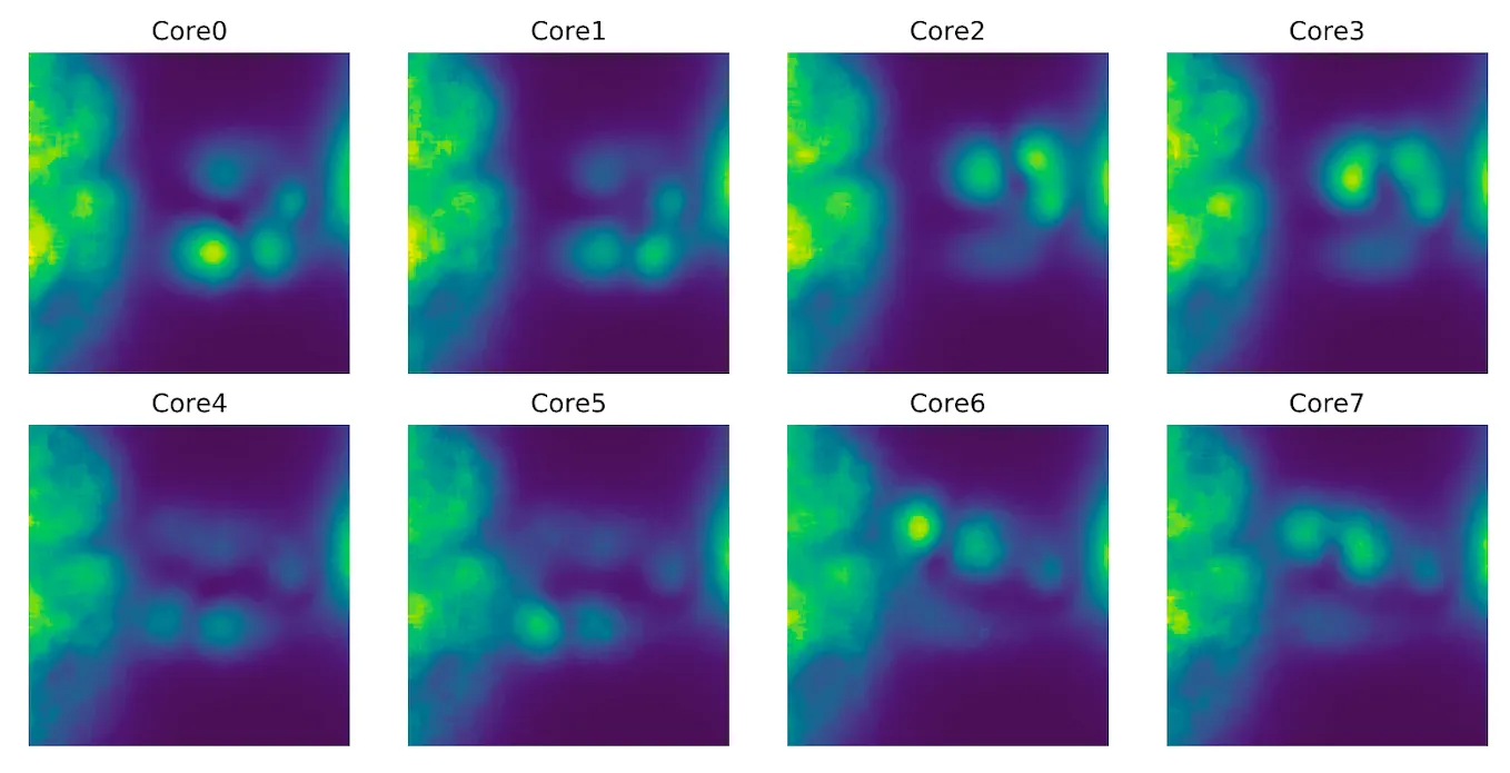
Figure - EM Cartography with AES running on each core.
But a more interesting observation is that some cores, such as 0, 3 or 6 seem to have a higher signal emission.
So far, from the signal observation it comes out that each core does not provide the same emission, some leak more than other, and also devices in the near proximity and involved in the processing can bring their contribution. While DRAM contribution was expected, the PMIC contribution is more surprising for the layman. This signal analysis provides us with probe positions to select the contribution of a given core.
It is time to focus on a core with the identified best probe position to collect side-channel signal and continue in deep the signal analysis.
When the probe is located on the active core, and the device operating an ECB encryption, each AES Activity is clearly visible, as shown on the following Figure. Showing that, we guess that exploitation of the signal should be easy.
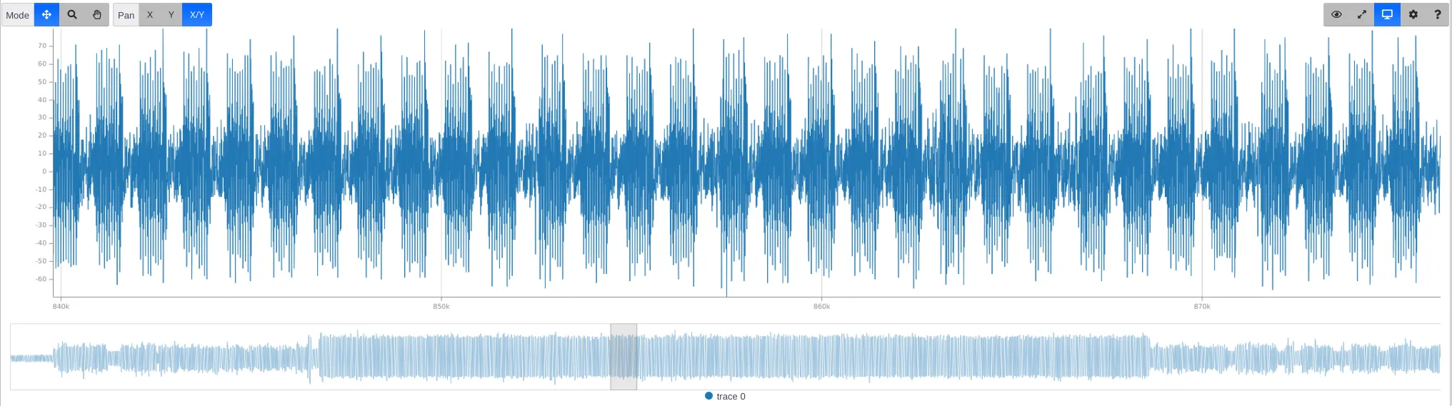
Figure - AES Activity clearly visible in ECB Mode without pipelining.
But in CBC mode, distinguishing AES becomes more handy… When AES is pipelined, the area corresponding to 1,000 AES is 1/3 compared to ECB not pipelined:
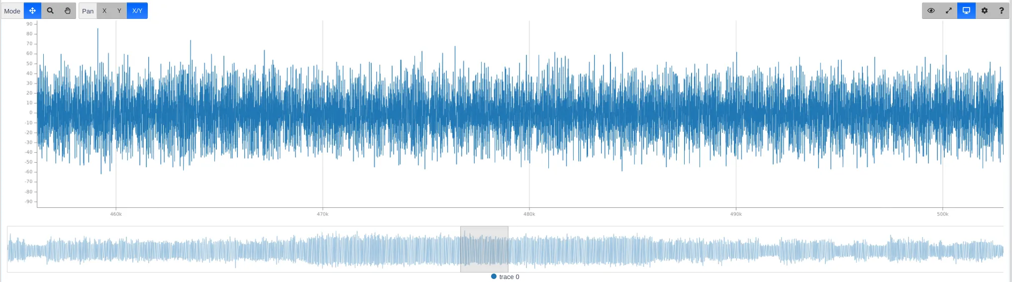
Figure - AES Activity in ECB and pipelined is much difficult to catch.
Waouh! We need to simplify the picture! In order to do so, we developed our own assembly codes using directly the ARMv8 AES instructions to operate the AES encryption or decryption without going through a library and have a full control of the execution context. With this bare-metal code, we will be able to evaluate the pipeline effect.
Before presenting these results, I was curious to look at the effect of some elements that may have a significant impact on the signal acquisition. I am talking about the elements related to micro-architecture.
From the micro-architecture standpoint, there are several factors that can modify and perturb the acquired signal quite significantly.
taskset <mask> <program>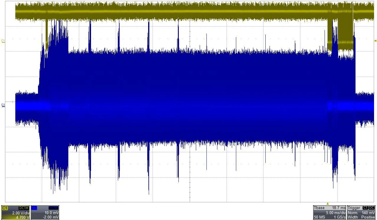
Figure - Signal with an interrupt every 4ms.
You can see that the duration of the interruption is decreasing more and more, probably because the task is directly rescheduled. Also, note that the execution core, if not set, can be modified after rescheduling.
As the high level API of OpenSSL is used, the code simply asks to encrypt a buffer in memory, and write the result in another buffer. But at a micro-architectural level, the SoC will have to preload and cache input memory, flush the cache lines that are not used anymore, and write back the data in upper memory layers.
If you are interested in very precise information about the timing of the Cortex-A53 CPU, you will find them in his report: https://www.7-cpu.com/cpu/Cortex-A53.html.
It is easy to identify L2 cache misses, because their duration is exactly 15 cycles + 128ns. We believe that L1 misses are sometimes visible, but other penalties such as branch misprediction are unlikely to happen in the middle of the cryptographic loop.
Below is an example of such penalties:
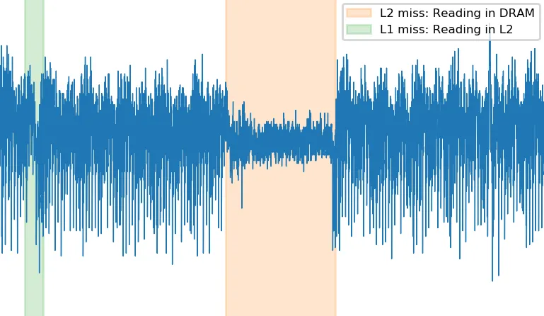
Figure A - Missing L2 Reading DRAM
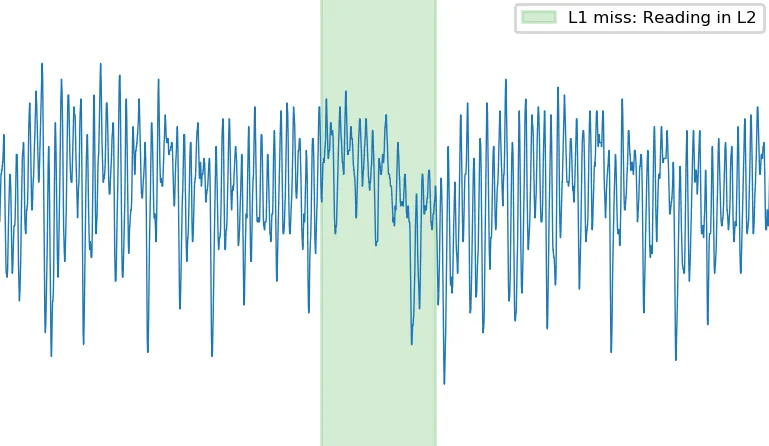
Figure B - Missing L2 Reading L1
Lastly, there are some areas, very close to the cores, that correspond to the cache activity. If the probe is located too close to these noise sources, you might end up with a signal that contains a pattern every 4 AES. It corresponds to the fetch/flush of a data line in L1 cache.
Below is an example of an EM signal that focuses on cache activity. This behavior can be more or less overlapped with the genuine core activity, but in any case, should be avoided.
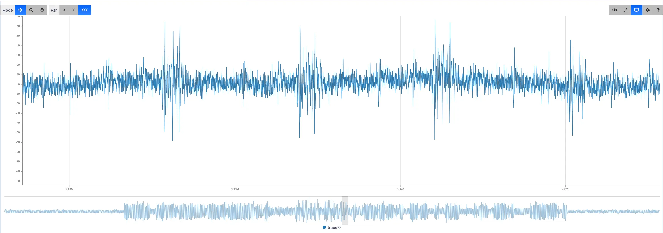
Figure - Zoom on Fetch/Flush of a data line in L1 cache during AES Activity.
Well, I’m sure you are curious about the effect of pipelining… As already mentioned, we have coded our own AES decryption using the ARMv8 cryptographic extension and the NEON 128-bit registers for the key and the data state. Thanks to this bare-metal approach we can perform acquisitions in a minimal environment: single-core up, no operating system, no external memory, etc. The purpose of this first study was to assess if ARM AES instructions were threatened by side-channel attacks.
Our code is the following:
func decrypt
        ldr     x3, =0xf9818010       // Pointer to input data
        ld1     { v0.16B }, [x3]      // Loading from memory to NEON register

        aesd    v0.16B, v11.16B       // First Round decrypt
        aesimc  v0.16B, v0.16B        // Inverse MixColumns
        aesd    v0.16B, v10.16B
        aesimc  v0.16B, v0.16B
        aesd    v0.16B, v9.16B
        aesimc  v0.16B, v0.16B
        aesd    v0.16B, v8.16B
        aesimc  v0.16B, v0.16B
        aesd    v0.16B, v7.16B
        aesimc  v0.16B, v0.16B
        aesd    v0.16B, v6.16B
        aesimc  v0.16B, v0.16B
        aesd    v0.16B, v5.16B
        aesimc  v0.16B, v0.16B
        aesd    v0.16B, v4.16B
        aesimc  v0.16B, v0.16B
        aesd    v0.16B, v3.16B
        aesimc  v0.16B, v0.16B
        aesd    v0.16B, v2.16B
        eor     v0.16B, v0.16B, v1.16B // Last AddRoundKey

        st1     { v0.16B }, [x3]       // Storing result in-place
        ret
endfunc decrypt
We captured a set of 100k traces with random messages and a single random, but known key. The obtained dataset was easy to synchronized with the basic pattern recognition technique, hereafter 10 traces after resynchronization:
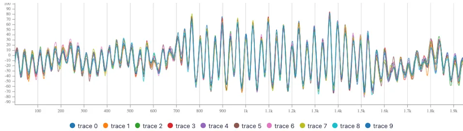
Figure - Bare-metal AES traces resynchronized.
In order to compare the attack results we rely on the guessing entropy computed at different step along the attack. On these figures we can only focus on the number of traces required for the SKEA strategy to reach 32 bit of remaining entropy corresponding to a realistic computation power.
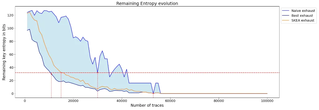
Figure - Guessing Entropy Result Bare-metal AES
So, as illustrated by these results, not pipelined AES execution is broken with around 15k traces when input and output of AES are known. If only the plaintext or the ciphertext is known, we found that around 50k traces are sufficient. This is far from what you can find in the literature [HA2022] that reports an attack with several tens of million traces! The encrypted image shown in the introduction is quite a big image and corresponds to only 230k 16-byte blocks. This makes decryption clearly out of reach of [HA2022], but within our reach!
Well, maybe the pipeline effect raises the bar …
To test this, we developed a code that interleaves three separated AES:
func decrypt_pipelined
        ldr x3, =0xf9818010         // Pointer to input data
        ld1 { v12.16B }, [x3], #16  // Loading from memory to NEON register
        ld1 { v13.16B }, [x3], #16  // 3 blocks at a time
        ld1 { v14.16B }, [x3], #16

        aesd    v12.16B, v11.16B    // Round 0
        aesimc  v12.16B, v12.16B
        aesd    v13.16B, v11.16B
        aesimc  v13.16B, v13.16B
        aesd    v14.16B, v11.16B
        aesimc  v14.16B, v14.16B

        aesd    v12.16B, v10.16B    // Round 1
        aesimc  v12.16B, v12.16B
        aesd    v13.16B, v10.16B
        aesimc  v13.16B, v13.16B
        aesd    v14.16B, v10.16B
        aesimc  v14.16B, v14.16B

        .../...

        aesd    v12.16B, v3.16B
        aesimc  v12.16B, v12.16B
        aesd    v13.16B, v3.16B
        aesimc  v13.16B, v13.16B
        aesd    v14.16B, v3.16B
        aesimc  v14.16B, v14.16B

        aesd    v12.16B, v2.16B     // Last Round
        aesd    v13.16B, v2.16B
        aesd    v14.16B, v2.16B
        eor     v12.16B, v12.16B, v1.16B
        eor     v13.16B, v13.16B, v1.16B
        eor     v14.16B, v14.16B, v1.16B

        ldr x3, =0xf9818010         // Reload pointer
        st1 { v12.16B }, [x3], #16  // Storing result in-place
        st1 { v13.16B }, [x3], #16
        st1 { v14.16B }, [x3], #16
        ret
endfunc decrypt_pipelined
After acquisition and straightforward synchronization, we get the following remaining entropy figure:
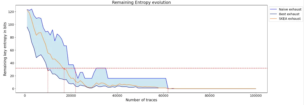
Figure - Guessing Entropy Result Bare-metal AES with pipeline, targeting first AES.
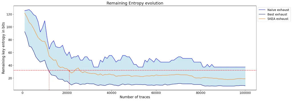
Figure - Guessing Entropy Result Bare-metal AES with pipeline, targeting Second AES.
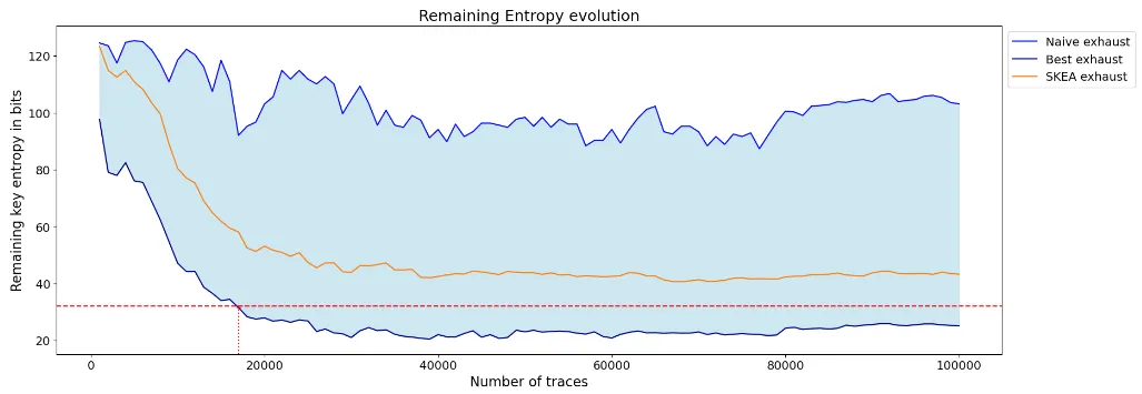
Figure - Guessing Entropy Result Bare-metal AES with pipeline, targeting Third AES.
So, targeting first, second or third AES clearly does not lead to the same result and one may conclude that pipelining can be a good direction for mitigation. But in the bag of selection functions an attacker has many choices… With a proper leakage analysis (performed knowing the key) we identified rapidly some selection functions voiding all the hopes:
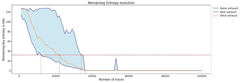
Figure - Guessing Entropy Result Bare-metal AES with pipeline, targeting Third AES.
Further investigations and attack refinements should be necessary to overcome micro-architectural effect and retrieve the AES secret key in an application context. We drove this analysis on several SoCs featuring the ArmV8 AES dedicated instructions and on each device, even with advanced technology (14nm), and with higher operating speed (1.8 Ghz) the results are very similar.
Clearly without mitigation the ARMv8 AES instructions does not offer a secure encryption.
If your application relies on the ARMv8 dedicated AES instructions, mitigation techniques will really make encryption time and power consuming, so that you will certainly not five star the encryption application. Indeed, these hardwired operators are not prone to deploy masking counter-measures. The remaining way, to make attacker life more difficult, is to lower the Signal to Noise Ratio (SNR). But, in view of our results, the mitigation will have a significant impact on the performance. As a side effect, it will also require careful code development, and will result in an increase of the code complexity. Moreover, these mitigation techniques will certainly not counter more advanced attacks like SCATTER [TGWC17] or attacks leveraging deep learning techniques c.f. [Mag]for instance.
Happily, for IoT and Mobile applications, there are cryptographic hardware solutions on the market providing a much higher resistance to side-channel attacks. So, with the proper choice of the SoC, it is possible to work around the weakness pointed here without performance penalty.
The results shared in this blogpost highlighted that a single photo decryption provides enough data to expose a secret key using a side-channel attack. The target concerns one of the cryptography resources available on many mobile or IoT devices: the ARM hardware implementation of an AES. The identification takes a bit of time since it has to compose with the complexity of a SoC, implementing cache, multiple cores, pipelining,…) and a rich OS. Once this complexity waved, the practicality turns out to be accessible for a limited cost.
Many things can be learned out of this analysis. First, ARM did not provide an algorithm intrinsically resistant to side-channel. Unless there is a rework by the semiconductor provider, the implementation cannot be deemed resistant. This means that any developer should consciously look at the hardware resources to perform sensitive operations and consider specific hardware accelerators claiming resistance to side-channel. This is confirmed by ARM’s answer to our responsible disclosure, stating that mitigations are in the scope of their silicon partners. One single photo for a secret key. How can Android developers consciously choose their crypto hardware resource? This is just another story for a future post!

Figure - Decrypted image.
2021-02-04: Vulnerability reported to ARM with description of the results obtained with both side-channel and laser fault injection. We indicate the platform used for our analysis.
2021-02-04: ARM security team (arm-security@arm.com) acknowledged reception and proper decryption of the report.
2021-03-17: After a month without news, we sent a kind reminder email but no answer.
2022-04-14: One year later, new remainder from our side…
2022-04-14: Arm security team answer that apologized for the long silence, hereafter the answer on the vulnerability:
We did discuss this issue internally, and our conclusion was that while power side channel attacks such as you describe are possible, they are not directly caused by or related to the Arm architecture. We’ve encouraged our silicon partners as part of general hardware and software design practices to provide both physical and software mitigations (such as timing invariant libraries). We’re working on an FAQ around these type of attacks, and will publish that FAQ shortly.
[HA2022] G. Haas, A. Aysu, Apple vs. EMA: Electromagnetic Side Channel Attack on Apple CoreCrypto PDF.
[ARMv8] ARM Holdings. 2021. Arm® Architecture Reference Manual Armv8, for Armv8-A architecture profile. (2021).
[TGWC17] H. Thiebeauld, G. Gagnerot, A. Wurcker, and C. Clavier. SCATTER : A New Dimension in Side-ChannelPDF
[Mag20] H. Maghrebi, Deep Learning based Side-Channel Attack: a New Profiling Methodology based on Multi-Label Classification


